Creating Boards from Scratch | ||||
|
| |||
It creates the board behavior.
Draw the outline of the board.
To do so:
-
Click Sketch
 ..
.. - Click Profile
 .
. - Sketch the contour of the board.
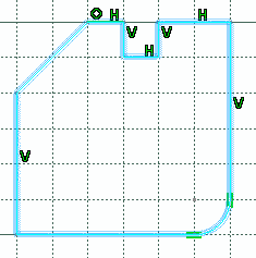
For more information about sketching profiles, refer to Sketching Simple Profiles in the Sketcher User's Guide: User Tasks.Tip: Sketch the outlines of any pockets directly at this stage. Note: You can also use a 3D curve for the board contour. However, if you want to export the board, you must define an axis system. For more information, see Export.
- Click Exit
 workbench to exit the Sketcher and return to Circuit Board Design.
-
Click Sketch
Create the shape for the board.
To do so:
- Click Pad
 .
.The Pad Definition dialog box appears.
The pad turns green; the board shape has been created. The board has been created from the active part.
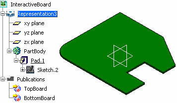
By default, CATIA recognizes the first pad created as the board.
You can add holes, pockets and constraint areas, as well as technological properties.
Important: A solid internal import, a generic solid feature (or a solid feature linked to a Part extended as Board / Panel) is not a valid Circuit Board Design entity. Thus, Circuit Board Design commands are not applicable for such entities. For more information, please refer to Part Design User's Guide: Handling 3D Shapes: Editing Copy / Paste Body Link. - Click Pad