Creating Constraint Areas | |||
| |||
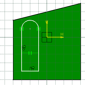
Draw the outline of the constraint area.
To do so:
- Click Sketch
 .
. - Select the board to define the working plane.
- Click Profile
 and draw a contour for the constraint area.
- Click Exit workbench
 to return to Circuit Board Design.
Note: You can also use a 3D curve for the outline. However, if you want to export the constraint area, you must define an axis system.
For more information, see Export.
- Click Sketch
Create the shape for the constraint area.
To do so :
Click Constraint Area
 .
.The Constraint Areas dialog box opens.
Constraint area types are:
- ROUTE_OUTLINE: An area on the board or panel where routing electrical connections is allowed.
- PLACE_OUTLINE: An area on the board or panel within which component placement is allowed.
- OTHER_OUTLINE: Additional area type defined by an outline, cutouts and a thickness.
- VIA_KEEPOUT: An area on the board or panel within which placement of vias is not allowed.
- PLACE_KEEPOUT: An area on the board or panel where component height is limited.
- PLACE_REGION: An area on the board or panel within which placement is limited to certain types of component.
- ROUTE_KEEPOUT: An area on the board or panel where routing electrical connections is not allowed.
Tip: To Graphic for the different types of constraint area, select Tools > Options... > Equipment & Systems > Circuit Board Design > Graphic and set the default color. Select PLACE_KEEPOUT and click OK.
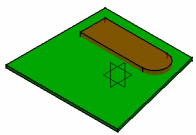
Constraint areas are transparent. The color depends on the type selected. The color can be changed in Graphic.
Constraint areas are grouped by type in the specification tree.
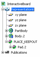
Note: The pad is more than a simple pad. It has technological properties.
 .
.